Another use of a micromachining laser
With the help of a very focused beam, it is possible to find application in microscopic areas as well. This is the machining of materials where the thickness does not exceed 1 mm and the machining must be performed with an accuracy of micrometers.
In this case, the focused beam is only a few micrometers in size, and in contrast to the use in mechanical welding, such devices must be very well controlled to achieve high accuracy. For small thermal effects at the machining site, it is necessary to use lasers with very short pulses, but with huge peak powers.
The most sought-after operations in laser micromachining include micro-cutting, micro-perforation, scribing, and selective material removal.
Micro cutting and scribing
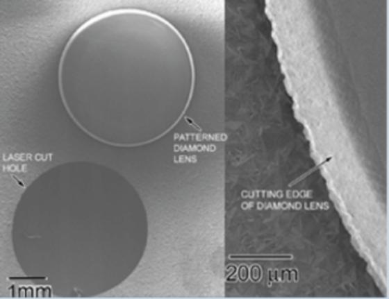
These applications include cutting diamond, silicon wafers, sapphire, ceramics and more.

Microdrilling
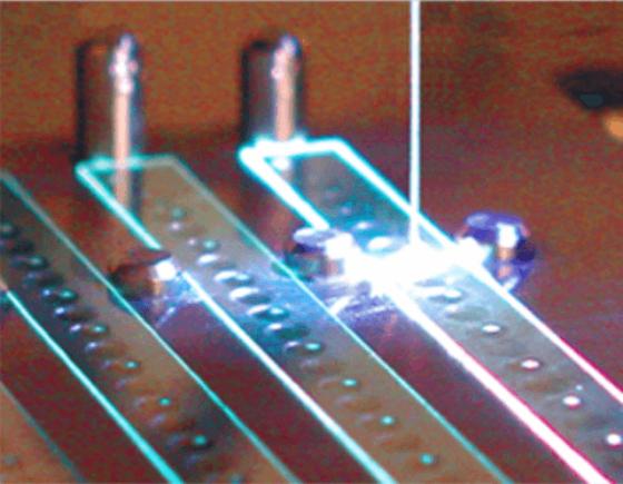
During micro-drilling, the holes are either through or dead-end, depending on the requirements. The holes can be only 2 microns wide and the punching speed can reach up to 1000 holes / s. Micro-drilling can be performed on a wide range of materials such as ceramics, metals, glass, polymers, and others.

Selective removal of materials
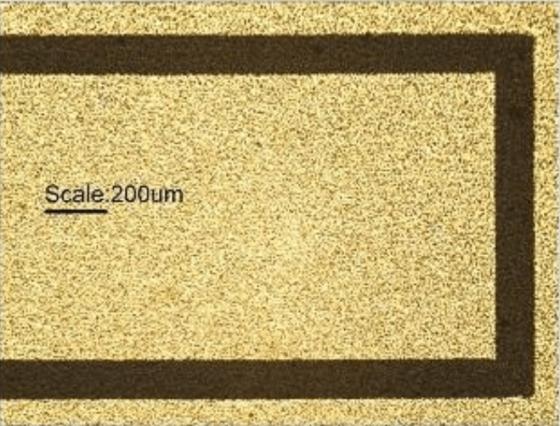
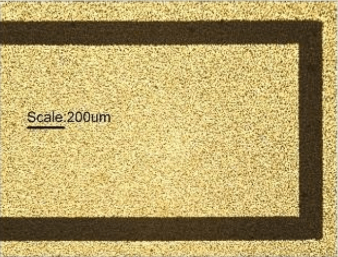
With the development of microelectronics, the aerospace industry and the automotive industry, the requirement for miniaturization is quite common. This applies not only to the smallest possible mechanical components but also to electronics. In these industries, it is necessary to fit a large amount of electronics into the smallest possible space. Therefore, the field of microelectronics is increasingly in demand. For the smallest possible dimensions of electronic components, the removal of conductive or insulating material on the substrate is used. In the past, a mask was used before applying a layer in the form of a tape or a small film, and unwanted debris in certain places was removed by etching. Laser layer removal in microelectronics is a good alternative to this traditional procedure. The use of laser technology in layer removal has brought with it speed, efficiency and accuracy. If more electrical circuit designs need to be made on a PCB, laser technology is a very successful method of achieving this.
A large variety of objects can be laser removed without disturbing the substrate or other layer below the unwanted layer. This involves the removal of layers of metals, ITO layers, or gold, copper, etc.
Ultrathin marking
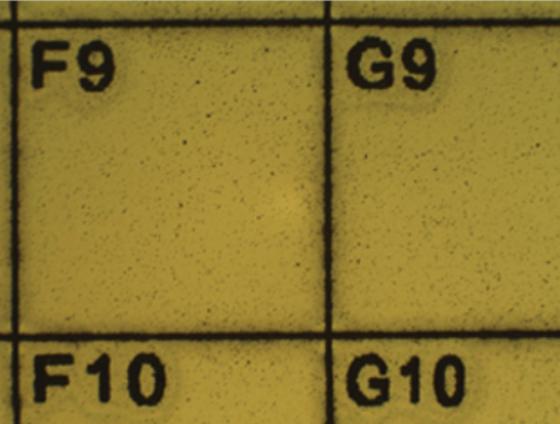
Currently, the demand for very small but high-quality markings is growing in various and transparent materials such as diamond, glass, ceramics, semiconductors and others. The size of the marking can be as small as 50 x 50um

Lasers suitable for micromachining
